Why Is PCB Manufacturing Equipment Important?

Why Is PCB Manufacturing Equipment Important?

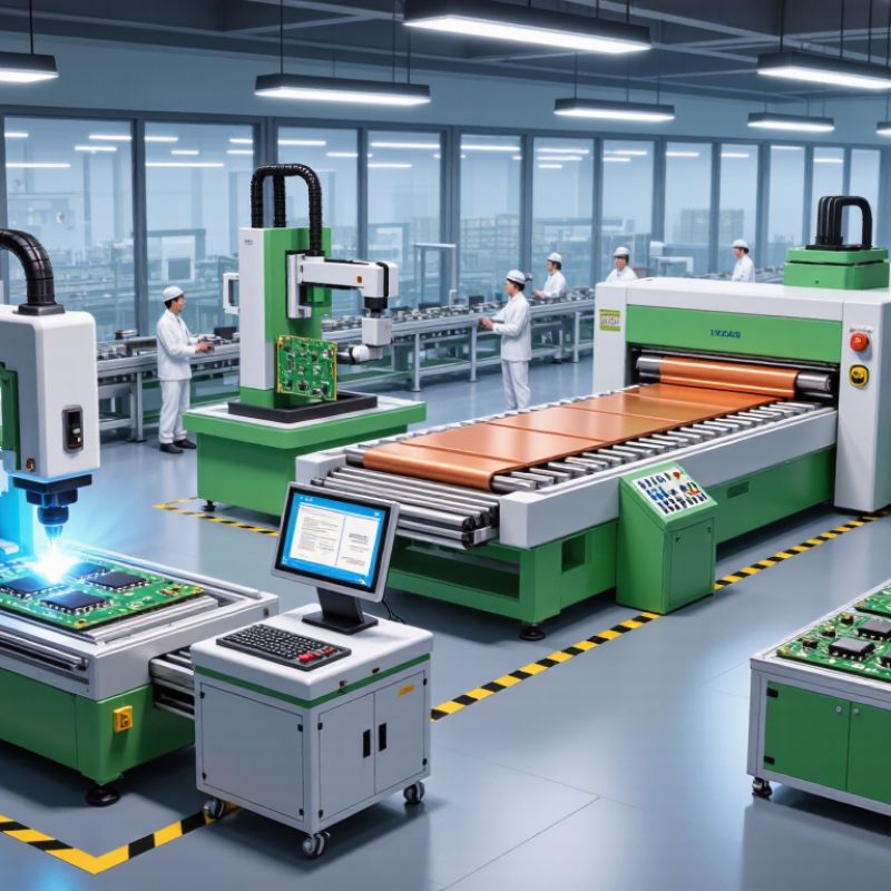
A printed circuit board may look simple: copper paths, small pads, and a green or blue surface. Producing it consistently is not simple. Each board passes through controlled steps, from imaging and etching to drilling, plating, and inspection. PCB manufacturing equipment makes those steps repeatable. It helps manufacturers place patterns accurately, remove unwanted copper, form reliable holes, and detect defects before boards reach assembly.

The machines matter because small errors can travel. A misaligned layer, rough hole wall, or uneven copper deposit can affect electrical performance or reduce production yield. Imaging systems, CNC drilling machines, lamination presses, and automated optical inspection tools each address different risks. Their value depends on more than speed. Calibration, maintenance, material choice, and operator skill all shape the final result. A fast machine is not automatically a reliable one.

Good equipment also supports traceability and process control. Sensors and inspection records can help teams compare batches and investigate recurring defects. Still, no machine removes every uncertainty. Materials vary, settings drift, and inspection methods have limits. That part is easy to overlook. Manufacturers need to match equipment to board complexity, volume, tolerances, and budget, then verify performance with real production data. Understanding why pcb manufacturing equipment matters is therefore useful for engineers, purchasing teams, and anyone evaluating board quality. The equipment is not merely factory hardware; it is part of the process that turns a design file into a dependable physical component.
Why Is PCB Manufacturing Equipment Important?

What PCB Manufacturing Equipment Includes and How It Works

Why Is PCB Manufacturing Equipment Important?

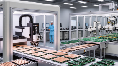
PCB manufacturing equipment turns a circuit design into a stable, usable board. The process begins with material preparation, cutting, and drilling. Computer-controlled drilling machines create precise holes for components and electrical connections. Small errors here can weaken the entire board.

Imaging equipment transfers the circuit pattern onto a copper-coated panel. Etching removes unwanted copper, leaving the required conductive paths. Plating equipment then strengthens holes and surface connections with controlled metal layers. Solder mask coating protects exposed copper and helps prevent accidental bridges during assembly. Screen printing or dispensing systems can add labels and solder paste with measured accuracy.

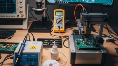
Inspection equipment is equally important. Automated optical inspection checks line width, missing copper, and surface defects. Electrical testers confirm whether each circuit carries current correctly. Experienced technicians still review unusual results because software can miss context. Calibration, temperature control, ventilation, and regular cleaning also affect production quality. From a production-floor perspective, equipment works as a connected system, not as isolated machines. One poorly maintained stage may damage later results. No setup is flawless. I have found that speed can hide quality problems when operators trust settings without checking samples. Careful records, sample testing, and practical judgment make the process more reliable.
Why PCB Manufacturing Equipment Matters

Equipment controls critical production steps—from laminating copper-clad material to drilling and plating holes. Accurate process control helps produce reliable copper layers and electrical connections.

Copper foil weight is commonly expressed in ounces per square foot. Approximate nominal thicknesses are 17.1 µm for 0.5 oz, 34.1 µm for 1 oz, and 68.3 µm for 2 oz copper.

How Equipment Supports Accurate PCB Production

Accurate PCB production depends on machines holding tiny features in position, repeatedly. A drilling system must keep each hole aligned with its design coordinates; imaging and etching equipment must preserve narrow traces without bridging them. Even slight variation can affect fit, electrical continuity, or yield. Automated optical inspection then checks for issues such as scratches, shorts, and incomplete traces. It helps catch defects, but it cannot correct a poorly controlled process.

Equipment capability matters most when it is measured and maintained. Calibration, clean optics, stable temperatures, and consistent material handling all support repeatable results. The International Federation of Robotics’ World Robotics 2023 report recorded 553,052 industrial robot installations worldwide in 2022, up 5% from 2021. That figure covers many industries, not PCB production alone. It does, however, show how widely automation is being adopted. IPC-6012 also sets performance and acceptance requirements for rigid printed boards, giving manufacturers defined criteria to check. A machine’s specifications are not a guarantee. Real production still depends on setup, inspection, and operator judgment; even experienced teams sometimes find that a process needs adjustment after the first panels are tested.

Why Automated Machinery Improves Manufacturing Efficiency

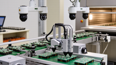
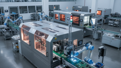
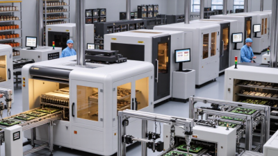
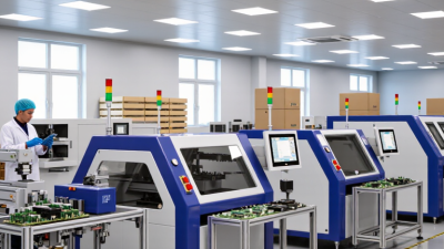
Automated machinery improves PCB manufacturing efficiency by reducing pauses between precise, repeatable tasks. A pick-and-place line can position components from feeder reels while cameras check board fiducials. The next panel moves along a controlled conveyor, rather than waiting for manual handling. Small gains across placement, soldering, and inspection can increase useful production time.

Consistency matters as much as speed. Automated solder-paste inspection can flag uneven deposits before boards reach reflow, where heat profiles affect joint quality. Optical inspection can then identify misplaced parts or visible solder defects. These checks give operators specific data to investigate, instead of relying only on end-of-line failures. Less guesswork. Fewer avoidable repeats.

Automation is not magic. A poorly loaded feeder, dirty camera lens, or incorrect setup can stop a line or reproduce the same defect across many boards. Skilled technicians still need to verify changeovers, review inspection results, and maintain equipment. Some processes also require manual adjustments for unusual board shapes or low-volume runs. The best efficiency comes from well-calibrated machines, clear work instructions, and people who know when the system’s output deserves a closer look.

How Equipment Ensures PCB Quality and Reliability

PCB quality is built into each process, not added at final inspection. A stable imaging system keeps copper traces aligned; controlled etching protects their width. Laser drills and plated-through-hole lines must hold consistent dimensions, or a tiny defect can interrupt a connection. On assembly lines, solder-paste inspection, reflow-oven profiling, and automated optical inspection catch different failure modes. X-ray inspection can reveal hidden solder joints. Small details matter.

Equipment also makes process variation visible. Calibrated sensors track temperature, pressure, registration, and test results across production runs. Deloitte and MAPI’s 2024 Smart Manufacturing Survey found that 86% of manufacturers saw smart manufacturing as a key competitiveness driver over the next five years. That finding is not PCB-specific, but it underscores the value of connected process data. IPC standards, including IPC-6012 and IPC-A-600, provide acceptance criteria for rigid boards and visual quality. Still, inspection is not magic. A camera may miss a defect outside its view, and a test fixture can drift if calibration is neglected. Good equipment needs trained operators, maintenance, and honest review of recurring failures. One overlooked setup change can undo a careful process.

Why Is PCB Manufacturing Equipment Important? - How Equipment Ensures PCB Quality and Reliability

Equipment Manufacturing Stage Quality Risk Addressed How It Supports Quality Typical Verification Data
Laser direct imaging (LDI) system Circuit pattern imaging Misaligned, distorted, or poorly defined circuit features Transfers the circuit pattern onto photoresist using a controlled digital image and registered panel positioning. Layer-to-layer registration, line and space measurements, and imaging inspection results
CNC drilling machine Hole formation Incorrect hole position, damaged hole walls, or unsuitable hole diameter Uses programmed coordinates and controlled spindle operation to create component and via holes consistently. Hole diameter, positional accuracy, drill-break records, and hole-wall inspection
Plating line Copper plating and via metallization Insufficient or uneven copper thickness and unreliable electrical connections between layers Controls process conditions such as current, time, and solution chemistry to deposit copper on board surfaces and hole walls. Copper thickness measurements, plating process records, and microsection examination
Automated optical inspection (AOI) system Circuit-pattern inspection Opens, shorts, missing copper, or unwanted copper features Captures board images and compares circuit features with a reference design to flag potential defects for review. Defect type and location, inspection coverage, and confirmed defect results
Solder mask coating and exposure equipment Solder mask application and patterning Uneven coverage, misregistered openings, or exposed copper in unintended areas Applies and patterns the protective mask so intended solderable areas remain exposed while other conductors are covered. Mask registration, coverage inspection, and opening dimensions
Electrical test system Finished-board testing Open circuits or unintended short circuits Tests electrical connections against the board’s netlist using a fixture or probe-based method. Pass/fail results, detected net faults, and test coverage records
Automated optical measurement system Final dimensional inspection Out-of-tolerance board dimensions, slots, or feature locations Measures physical features against drawing requirements, supporting consistent fit and assembly. Board outline, hole and slot dimensions, and measurement records

The Role of Advanced Equipment in Future PCB Manufacturing

Why Is PCB Manufacturing Equipment Important?

The Role of Advanced Equipment in Future PCB Manufacturing

Advanced equipment is reshaping how future PCB factories control quality, speed, and waste. Modern imaging systems can detect narrow trace defects before boards reach assembly. Automated drilling platforms maintain hole positions within strict production tolerances. This matters when compact devices require dense interconnections and smaller manufacturing margins.

In practical production, equipment must do more than operate quickly. It should record temperature, pressure, tool wear, and inspection results during each batch. These records support traceability and help engineers identify repeated process changes. High-precision solder paste inspection can reveal uneven deposits around fine pads. Early detection prevents expensive rework and protects downstream reliability.

Still, advanced machinery is not a complete solution. Poor calibration can quietly damage an otherwise capable process. Operators need training, maintenance routines, and clear verification steps. Human judgment remains important when unusual surface marks confuse automated inspection. That part is easy to underestimate. Future factories may use more artificial intelligence, but engineers must question abnormal results instead of accepting every machine decision. In my view, the strongest manufacturing systems will combine measurable automation with experienced review, especially when material behavior changes between production runs.