What is the Process to Design Your Own Circuit Board?
Designing your own circuit board can seem daunting. However, it's an exciting journey for many engineers and hobbyists. According to Mark Smith, a leading expert in electronics design, “The true art of circuit design lies in understanding your purpose.” This statement reflects the idea that purpose drives creativity in electronic designs.
Creating a circuit board begins with a clear concept. You must know what functionality you desire. This clarity shapes your design choices. Draw schematics to visualize your ideas. Selecting components wisely is crucial; each choice impacts the final product. Debugging will be an ongoing challenge throughout the process and requires patience and attention to detail.
Finally, after laying out the design, it is time to produce the board. Manufacturers offer various options, which can be overwhelming. Errors in the design phase can lead to significant setbacks, reminding designers of the importance of precision. Reflecting on each step of the journey helps improve future designs. Embracing this learning process is vital when you decide to design your own circuit board.

Understanding the Basics of Circuit Board Design
Designing your own circuit board can be both exciting and daunting. Understanding the basics is crucial. Start by defining the purpose of your circuit. What do you want it to do? This clarity will guide your design decisions. Sketching your ideas on paper or using software helps visualize connections and components. Choose the right materials and tools as well.
Next, focus on component placement. Keep in mind the size of your board and the space required for components. It’s easy to make mistakes here. Make sure to check the distances and alignments. Often, when laying out a board, you might overlook simple details like trace width or clearance. This can lead to frustrating errors later.
After assembling your board, testing is vital. You may face issues that require revisiting your design. Reflection is necessary. What worked? What didn’t? This iterative process can be tough, but it sharpens your skills. Each revision brings you closer to a reliable circuit board. Embrace the challenges and learn from them.
Understanding the Basics of Circuit Board Design
This chart illustrates the key aspects of the circuit board design process, focusing on the essential phases involved in developing a new circuit board.
Choosing the Right Materials for Your Circuit Board
Choosing the right materials for your circuit board is crucial. The material affects performance, durability, and cost. Common choices include fiberglass and epoxy. These materials provide strong support for components, but can vary in price. Consider the heat resistance as well. Some applications require high-temperature handling.
Another important factor is the thickness of the board. Thicker boards can handle more stress but may be less flexible. This can limit your design options. Keep in mind that the manufacturing process can complicate material selection. Not all materials are easy to work with.
Surface finish also plays a key role. Different finishes affect solderability and corrosion resistance. Some may even require additional cleaning. Evaluate your needs carefully. It's important to test different combinations. This can lead to unexpected challenges. Reflect on your choices as you design. There’s always a balance to strike between cost and performance.
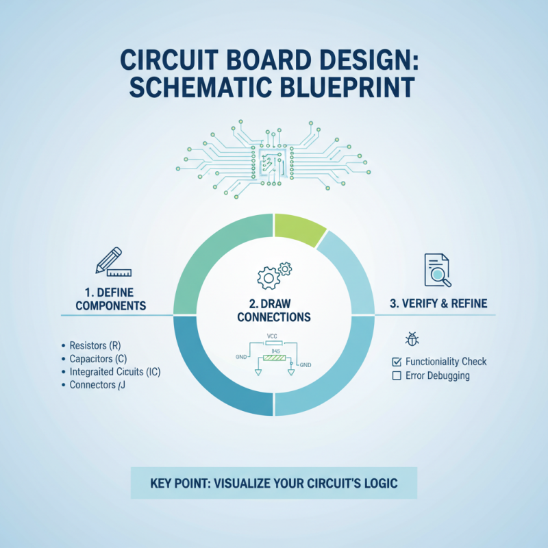
Steps to Create a Schematic Diagram
Creating a schematic diagram is a critical step in designing your own circuit board. This diagram acts as the blueprint for your circuit. Start by clearly defining the components you'll need. List resistors, capacitors, and any other elements. Keep this list simple, but detailed. Each component should have a specific role in your circuit.
Begin sketching your schematic with software tools. These tools simplify the layout of your components. Lay out the parts logically. Ensure wires do not cross unnecessarily. A cluttered diagram can lead to confusion later. While this may take time, clarity is vital.
**Tip:** Check your schematic multiple times. Small mistakes can cause big problems. If something looks off, re-evaluate. Sometimes, stepping away from your work helps you see errors.
Consider testing your schematic with simulations. It can reveal design issues before you begin fabrication. Don’t hesitate to seek feedback from peers. They might notice things you’ve missed. Collaboration can enhance the quality of your design.
**Tip:** Document every change you make. This record helps you track your decisions. It also serves as a valuable resource if you revisit your project later. Making mistakes is part of the learning curve. Embrace it.
Translating Schematics into PCB Layout
Translating schematics into PCB layout is vital in circuit board design. This process involves taking electronic circuit schematics and converting them into a format suitable for manufacturing. Accurate translation is essential. A study by IPC, an international trade association, found that improper layout can lead to a 30% increase in production costs.
During translation, engineers must consider various factors. The arrangement of components on the board affects signal integrity and thermal performance. This stage requires attention to detail. Mistakes, even minor, can result in malfunction. For instance, improper placement can lead to unintentional interference between components, which can cripple the entire circuit.
It's essential to use appropriate software tools. Many tools provide automated features, but human oversight remains crucial. Relying solely on automation can introduce errors. Reports indicate that nearly 20% of PCB prototypes fail due to layout issues. Regular reviews and revisions help mitigate this risk. Engaging multiple team members in this process can unveil potential problems early. Collaboration fosters creativity, enhancing the final product’s reliability and performance.
What is the Process to Design Your Own Circuit Board? - Translating Schematics into PCB Layout
| Step |
Description |
Tools Required |
Estimated Time |
| 1 |
Define the circuit requirements and specifications. |
Specification Sheet |
1-2 hours |
| 2 |
Create a schematic diagram of the circuit. |
Schematic Software (e.g., LTspice, Eagle) |
2-3 hours |
| 3 |
Convert the schematic into a PCB layout. |
PCB Design Software (e.g., KiCAD, Altium) |
3-4 hours |
| 4 |
Simulate the PCB to identify any design issues. |
Simulation Software |
1-2 hours |
| 5 |
Finalize the design and prepare for manufacturing. |
Design Rule Check Tools |
2 hours |
| 6 |
Order the PCB from a manufacturer. |
Online PCB Service |
1 hour |
| 7 |
Assemble and test the components on the PCB. |
Soldering Tools, Multimeter |
3-6 hours |
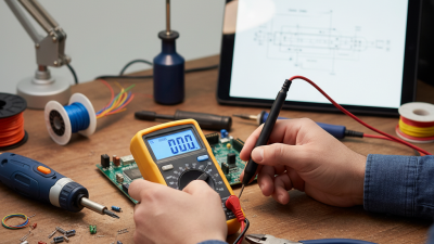
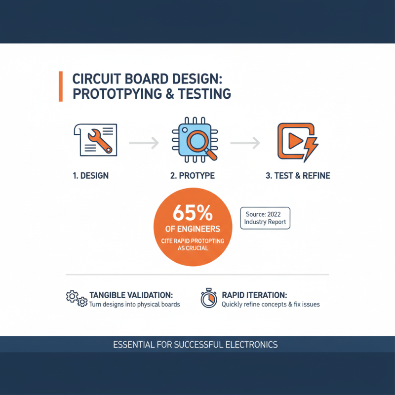
Prototyping and Testing Your Circuit Board Design
When designing your own circuit board, prototyping and testing play essential roles. The prototype phase transforms your design into a tangible entity. This process often involves creating a small batch of boards to validate your concepts. According to a 2022 industry report, 65% of engineers cite rapid prototyping as crucial for refining their designs.
However, prototyping is not without challenges. It’s common to encounter issues such as incorrect component placement or inadequate soldering. Statistics indicate that nearly 30% of prototype boards fail testing due to these errors. Addressing these flaws requires iteration and patience. Testing the circuit board under real conditions often unveils discrepancies in performance. For instance, voltage drops might occur unexpectedly, leading to functionality failures.
Reflecting on the prototyping process can uncover valuable insights. Spending time analyzing test results sheds light on design flaws, but it often requires multiple attempts. A survey from 2023 revealed that 70% of engineers admit to learning more from their failures during this phase than from their successes. Each test provides an opportunity to refine and enhance your design, pushing it closer to reliability and efficiency.