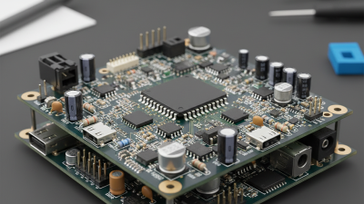
In 2026, make your own circuit board is more practical than ever. Affordable design software, desktop CNC machines, and reliable fabrication services have changed the learning process. A small electronics project can now move from a sketch to a tested board within days. However, success still depends on careful planning, not just modern tools.
This guide explores the complete process, from selecting components to creating a manufacturable PCB layout. You will learn how to define circuit requirements, place footprints, route traces, and check clearances before production. Practical details matter. A misplaced connector can make an enclosure useless. A thin trace may overheat under real current. A forgotten ground connection can stop an otherwise attractive design.
Mistakes are part of the work.
I have found that beginners often focus on appearance before electrical reliability. That approach needs reconsideration. A professional board should be easy to inspect, assemble, repair, and improve. Design rules should match the manufacturer’s capabilities, while safety precautions should guide soldering, testing, and power selection. Never test an unknown circuit beside flammable materials or unsupported power sources.
This introduction also considers engineering judgment. Simulation can reveal problems, but it cannot replace physical testing. Datasheets provide authority, yet real components may behave differently in a crowded enclosure. By combining documented research, measured results, and careful revision, you can build a circuit board that performs beyond the screen. The goal is not perfection on the first attempt. It is a dependable design shaped by evidence, patience, and honest reflection.

A successful circuit board begins with a narrow purpose, not a crowded parts list. Write one sentence describing its job, such as “measure room temperature every ten seconds.” Then record voltage, current, operating temperature, enclosure size, connectors, and expected service life. A 2024 global PCB market report estimated the market at about US$89.7 billion in 2023, with steady growth ahead. That scale reflects rising complexity, but a hobby design still needs disciplined requirements.
Turn requirements into a block diagram before drawing detailed symbols. Separate power input, regulation, processing, sensing, communication, and output stages. For a 12-volt motor controller, specify startup current, logic voltage, fuse rating, switching frequency, and heat limits. Add test points for ground, regulated voltage, and critical signals. Small details matter. A missing test point can turn a five-minute check into an hour of probing.
Draw the schematic using recognized symbols and clear net names. Follow the electrical-spacing and documentation principles in IPC-2221, then review polarity, unused pins, return paths, and connector orientation. I often leave a spare input and one extra mounting hole. That may seem wasteful. It has saved revisions. My early schematics also looked complete, yet ignored cable movement and connector strain. Review the drawing with real wires, screws, heat, and user mistakes in mind.
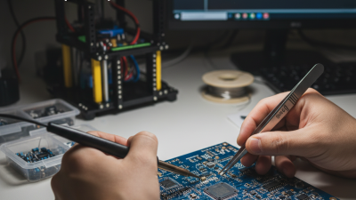
Choose materials that match your circuit’s voltage, current, and working environment. For most prototypes, two-layer FR-4 provides a stable and affordable base. Use copper thickness according to expected current, not guesswork. A wider trace reduces heating. Keep exposed copper protected with solder mask, especially near humid areas. For compact boards, surface-mount components save space, but through-hole parts are easier to inspect and replace. Choose components with available technical documents and clear tolerances.
Begin with a schematic, then convert it into a carefully checked PCB layout. A ground plane can reduce noise and simplify return paths. Keep sensitive signal traces away from switching or high-current sections.
Place connectors first, followed by large components and heat-producing parts. Check spacing, hole sizes, trace widths, and polarity marks before exporting manufacturing files.
Electrical and design-rule checks catch many mistakes, but they cannot judge every practical problem. My first layout passed software checks and still had an awkward connector position.
Tips: Print the board at full scale. Place real components on the paper. This simple test reveals surprising errors. Label test points clearly, and leave room for a probe tip. Keep a revision record for every change. Measure critical voltages after assembly, rather than trusting the design file alone. A small prototype may need two or three revisions. That is normal.
A reliable circuit board starts with a layout that matches the intended manufacturing process. Draw the schematic, define the board outline, then place connectors and large components before routing signals. Keep fast-changing signals short, separate noisy power paths from sensitive analog traces, and add a continuous ground plane where the stack-up allows. Small details matter. Check trace width, copper spacing, drill sizes, and solder-mask clearances against the fabricator’s published capabilities. IPC-2221 provides general guidance for printed-board design, but it does not replace a manufacturer’s specific rules.
Before release, create a stack-up and verify that the chosen material, copper weight, and finished thickness are available. Run design-rule checks, inspect the board in 3D, and review the Gerber files, drill data, and bill of materials together. One overlooked connector footprint can waste a whole prototype cycle. I still find that easy to miss. MarketsandMarkets’ 2024 PCB market report projects growth from USD 70.4 billion in 2024 to USD 90.7 billion by 2029; that forecast is not a design rule, but it reflects a growing need for buildable boards. Send the fabricator clear notes on impedance, controlled tolerances, and any unusual process requirements. Then request a manufacturability review before ordering.
| Step | Design Stage | Key Actions | Manufacturing Checks | Typical Output |
|---|---|---|---|---|
| 1 | Define requirements | Document the board’s purpose, interfaces, operating voltage, expected current, environment, and size limits. | Confirm that component choices and electrical requirements are compatible with the intended use. | Requirements list and preliminary block diagram |
| 2 | Create the schematic | Choose components, connect circuit symbols, assign reference designators, and add power and ground connections. | Run electrical-rule checks and verify that footprints are available for every physical component. | Schematic and initial bill of materials |
| 3 | Set board constraints | Choose the board outline, number of copper layers, material, copper weight, and design-rule limits. | Compare minimum trace width, spacing, drill size, and layer stack-up with the fabricator’s published capabilities. | Board outline and constraint profile |
| 4 | Place components | Arrange connectors, mechanical features, heat-producing parts, and other components according to signal flow and access needs. | Check clearances, polarity markings, component orientation, mounting holes, and enclosure fit. | Preliminary component placement |
| 5 | Route the board | Route signal, power, and ground connections; use suitable copper widths and planes for current and return paths. | Review high-speed paths, loop areas, via use, thermal reliefs, and spacing against the chosen design rules. | Routed copper layers |
| 6 | Review layout and silkscreen | Add readable reference labels, polarity indicators, test points, and assembly notes without obscuring pads or openings. | Run design-rule checks and inspect the board in 2D and 3D for overlaps, unconnected nets, and mechanical conflicts. | Reviewed PCB layout |
| 7 | Prepare manufacturing files | Generate copper, solder-mask, silkscreen, and board-outline Gerber files, plus Excellon drill files. | Check file units, layer names, drill plating information, board dimensions, and alignment before submission. | Gerber and drill package |
| 8 | Verify and release | Review the exported files in an independent viewer and prepare assembly data if components will be fitted. | Confirm the fabrication notes, stack-up, finish, panelization requirements, and bill-of-materials details. | Manufacturing-ready design package |
Making a circuit board in 2026 starts with a clean schematic and realistic tolerances. IPC’s 2024 economic outlook projected roughly 5% growth for the global electronics industry. That growth increases demand for small, reliable boards.
Cut copper-clad laminate to size. Mark the drilling points with a sharp carbide bit. Transfer the circuit pattern using toner transfer or a photoresist film. Keep traces wide enough for your expected current. Fine traces look impressive, but they punish small alignment errors. Etch the exposed copper in a ventilated workspace. Wear eye protection and gloves. Follow local rules for chemical storage and disposal. Rinse the board thoroughly, then inspect every track under bright light. One overlooked bridge can ruin the entire board.
Drill component holes slowly. Remove burrs before soldering. Apply flux sparingly. Install low-profile parts first, then taller components. This keeps the board stable during assembly. IPC’s J-STD-001 standard emphasizes solder quality, cleanliness, and controlled heating. A practical target is a bright, smooth joint with complete wetting. Do not trust appearance alone. Check continuity with a multimeter before applying power. My first boards often failed because I skipped this step. That mistake still feels embarrassing.
For surface-mount parts, use a stencil and a controlled hot plate or reflow method. Measure temperature carefully. A 2024 industry survey from IPC reported continuing pressure for higher manufacturing quality and faster delivery, but home fabrication remains less predictable. Document failed traces, reversed diodes, and weak joints. That record becomes your real process guide.
After making your circuit board, inspect every joint under bright, angled light. Look for dull solder, bridges, lifted pads, and tiny cracks around component leads. Compare the finished board with your schematic and layout before applying power. Check polarity marks carefully. A reversed diode or capacitor can damage the board quickly.
Tips: Keep the board clean and dry. Use a pointed probe for continuity checks. Test between power and ground first. Record each measurement, even when it seems obvious. Do not rely only on visual inspection.
Solder joints should appear smooth and firmly connected, not excessively large. Touch up weak joints with controlled heat, then let the board cool. I still occasionally miss a small bridge near closely spaced pins. That is a useful reminder to inspect twice.
Use a multimeter to verify resistance, continuity, and supply voltage. Power the board through a current-limited source when possible. Watch for unexpected heat, smell, or current rise, and disconnect power immediately if they appear.
Test one section at a time, such as the power circuit before the signal path. If the board fails, check connectors, ground paths, solder bridges, and incorrect component values. A simple fault log makes repeated testing more reliable.
Never guess for long. Measure again.